


Flying Probe Test
QCG provides in-house flying probe test and supports developing test procedures as well as implementing existing programs. As part of our continuing improvement QCG has developed new software and techniques to reduce the amount of time necessary to program and debug tests.
Flying probe test is not just for finding manufacturing errors. It is an excellent prototyping support tool that can significantly reduce engineering bring-up by verifying power rails, detecting schematic errors and checking resistor values/tolerances. Sophisticated algorithms in the tester compensate for in-circuit values of resistance, capacitance and inductance providing the test technician with intuitive information that is provided to the hardware engineer before power is applied to the board.
Flying probe test combined with strategic boundary scan and/or functional test is an excellent low cost alternative to expensive an ICT (In-circuit Test) bed of nails fixture.
Design for Test
(DFT)
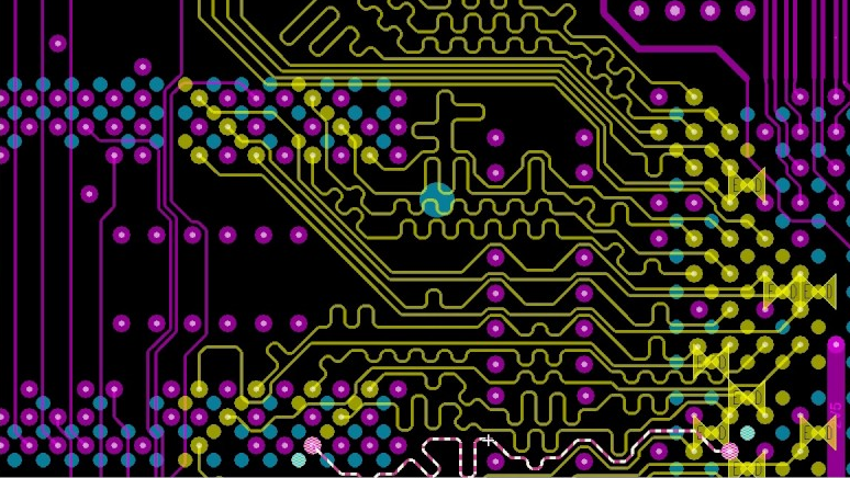
Maximum flying probe test coverage begins with the PCB layout. The majority of CAD tools come equipped with built in DFT support to turn existing vias into probable test points. To ensure the best coverage, vias that are exposed to surface layers (non- buried vias) should not be covered with soldermask. In addition to test point pads that are designed into the PCB, the machine is able to probe both vias and components pads as well.
Functional Test Development
QCG can develop fully automated test fixtures that include test procedure generation on LabView, Windows, UNIX and Linux platforms. We support both unit and system level applications for in-house verification of assembled products.
Boundary Scan
JTAG IEEE boundary scan test 1149.1 and IEEE 1149.4. Our engineers can evaluate your schematic to assist in developing an efficient boundary scan test. Reduce or eliminate the need for test points that can negatively affect signal integrity on high-speed circuits. Boundary scan can cover places that physical probes cannot access due to board density or components with inaccessible leads such as BGAs.